1. What is SDRAM ?
SDRAM is high-speed Dynamic Random Access Memory (DRAM) with a synchronous interface. The synchronous interface and fully pipelined internal architecture of SDRAM allow extremely fast data rates if used efficiently. SDRAM is organized in banks of memory addressed by row and column. The number of row and column address bits depends on the size and configuration of the memory. Synchronous meaning there will be a clock and data relationship.
2. How data is written and read in the SDRAM?
The memory cell is written to by placing a “1” or “0” charge into the capacitor cell. This is done during a write cycle by opening the cell transistor (gate to power supply or VCC) and presenting either VCC or 0V (ground) at the capacitor. The word line (gate of the transistor) is then held at ground to isolate the capacitor charge. This capacitor will be accessed for either a new write, a read, or a refresh.
3. How Row Address and Column Address access happen in SDRAM ?
First Step: Row Addresses Row addresses are present on address pads and are internally validated by the RAS (Row Address Access) clock. A bar on top of the signal name means this signal is active when it is at a low level. The X addresses select one row through the row decode, while all the other non-selected rows remain at 0V. Each cell of the selected row is tied to a sense amplifier. A sense amplifier is a circuit that is able to recognize if a charge has been loaded into the capacitor of the memory cell, and to translate this charge or lack of charge into a 1 or 0. There are as many sense amplifiers as there are cells on a row. Each sense amplifier is connected to a column (Y address). In this first step all the cells of the entire row are read by the sense amplifier. This step is long and critical because the row has a high time constant due to the fact that it is formed by the gates of the memory cells. Also, the sense amplifier has to read a very weak charge (approximately 30 femtoFarads or 30fF).
Second Step: Column Addresses Following the first step, column addresses are present on the address pads and are internally validated by the Column Address Access (CAS) clock. Each selected memory cell has its data validated in a sense amplifier. Column access is fast. This step consists of transferring data present in the sense amplifier to the Dout pin through the column decode and the output buffer. On memory data sheets, the access time from RAS is termed tRAC and the access time from CAS is listed as tCAC. On a typical standard DRAM of 60ns access time, tRAC = 60ns and tCAC = 15ns.
4. What refresh command does in SDRAM ?
The word “DRAM” is an acronym for Dynamic Random-Access Memory. The nature of the non- persistent charge storage in the DRAM cells means that the electrical charge stored in the storage capacitors will gradually leak out through the access transistors. Consequently, to maintain data integrity, data values stored in DRAM cells must be periodically read out and restored to their respective the DRAM the row address from the refresh address register and then sends the same row address to all banks to be refreshed concurrently. the single refresh command to all banks takes one refresh cycle time tRFC to complete
5. How Read cycle complete in SDRAM ?
Read get complete in three steps
1. Row access command
2. column read
3. Precharge
Each Row access command brings all the data bits to the array of sense amplifier in given bank . Then by the column access read command these data bits brings to the memory controller through data bus .
Then, after tRAS time from the initial issuance of the row access command, the DRAM cells are ready for a precharge command to reset the bitlines and the sense amplifi ers. Collectively, memory systems that immediately precharge a bank to prepare it for another access to a different row are known as close-page memory systems. Memory systems that keep rows active at the sense amplifi ers are known as open-page memory systems
6. Write cycle For DRAM ?
In the case of a write access, data must be provided by the memory controller, driven through the data bus, passed through the I/O gating multiplexors, overdrive the sense amplifi ers, and fi nally stored into the DRAM cells. This complex series of actions must be completed before the precharge
command that completes the sequence can proceed.
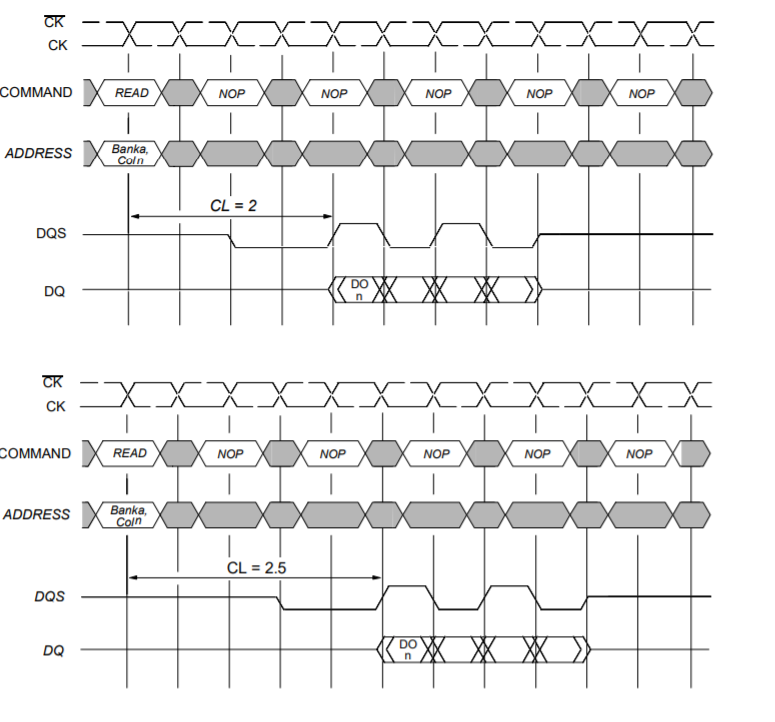
7. How DDR read command completed?
READ bursts are initiated with a READ command. The starting column and bank addresses are provided
with the READ command and AUTO PRECHARGE is
either enabled or disabled for that burst access. If
AUTO PRECHARGE is enabled, the row that is accessed
will start precharge at the completion of the
burst.
During READ bursts, the valid data--out element from
the starting column address will be available following
the CAS latency after the READ command. Each subsequent
data--out element will be valid nominally at the
next positive or negative clock edge (i.e., at the next
crossing of CK and CK). DQS is driven by the DDR
SDRAM along with output data. The initial LOW state
on DQS is known as the read preamble; the LOW state
coincident with the last data--out element is known as
the read postamble.
8. How DDR write command completed?
The WRITE command is used to initiate a burst write access to an active row. The value on the BA0, BA1 inputs selects the bank, and the address provided on inputs A0--Ai, selects the starting column location. The value on input A10 determines whether or not auto precharge is used. If auto precharge is selected, the row being accessed will be precharged at the end of the write burst; if auto precharge is not selected, the row will remain open for subsequent accesses. Input data appearing on the DQs is written to the memory array subject to the DM input logic level appearing coincident with the data. If a given DM signal is registered LOW, the corresponding data will be written to memory; if the DM signal is registered HIGH, the corresponding data inputs will be ignored, and a write will not be executed to that byte/ column location.
9. Why active command is Needed?
Activate command is used to active the ROW, without active, we can't do any read or write operation.
First, activate command issued, BA0-1 tell the bank info and A0-10 tell the ROW info, once the row is activated then only the row is ready for any kind of data transfer.
10 . What is the precharge command?
The precharge command completes the row access sequence as it resets the sense amplifi ers and the bitlines and prepares them for another row access command to the same array of DRAM cells
The two row-access-related timing parameters, tRP and tRAS, can be combined to form tRC, the row cycle time. The row cycle time of a given DRAM device denotes the minimum amount of time that a DRAM device needs to bring data from the DRAM cell arrays into the sense amplifi ers, restore the data to the DRAM cells, and precharge the bitlines to the reference voltage level for another row access command. The row cycle time is the fundamental limitation to the speed at which data can be retrieved from different rows within the same DRAM bank. As a result, tRC is also commonly referred to as the random row-cycle time of a DRAM device.
11. How AUTO PRECHARGE command is issued?
AUTO PRECHARGE is a feature which performs the same individual--bank precharge function described above, but without requiring an explicit command. This is accomplished by using A10 to enable AUTO PRECHARGE in conjunction with a specific READ or WRITE command.
12. Difference between auto refresh and self Refresh?
self-refresh mode is nothing but just a standby mode, so that data is not lost when external clock is not there.. it is purely to save power consumption.. CKE is high during the self refresh case .
DLL is automatically off and on based on the enter and exit of self refresh command .
Auto-refresh mode auto refreshing of data happens every pre-defined time intervals.. usually a command is there to enter self refreshing mode. To allow for improved efficiency in scheduling and
switching between tasks, some flexibility in the absolute
refresh interval is provided. A maximum of
eight AUTO REFRESH commands can be posted
to any given DDR SDRAM, and the maximum absolute
interval between any AUTO REFRESH command
and the next AUTO REFRESH command is
8 * tREFI.
13. what is ODT ?
On die termination ODT is typically required as the speeds increase into the DDR2 and DDR3 range. The
impedance of the ODT is typically a trade-off between signal integrity and power
consumption. In most cases, the Rtt value is slightly higher in comparison with the RON
value of the DRAM. By doing this, the signaling will not be as clean, but the gain in
voltage margin helps close timing. An even higher Rtt can be chosen to reduce power
like 150Ω. The real question comes down to whether it’s good enough to still close timing
and to burn as little power as possible.
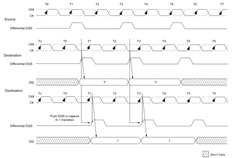
14. How write leveling is done ?
IFor better signal integrity, DDR3 SDRAM memory modules have adopted fly-by topology for the commands, addresses, control signals, and clocks. Write leveling is a scheme for the memory controller to adjust or de-skew the DQS strobe (DQS, DQS#) to CK relationship at the DRAM with a simple feedback feature provided by the DRAM. Write leveling is generally used as part of the initialization process, if required. For normal DRAM operation, this feature must be disabled. This is the only DRAM operation where the DQS functions as an input (to capture the incoming clock) and the DQ function as outputs (to report the state of the clock). Note that nonstandard ODT schemes are required.
The memory controller using the write leveling procedure must have adjustable delay settings on its DQS strobe to align the rising edge of DQS to the clock at the DRAM pins. This is accomplished when the DRAM asynchronously feeds back the CK status via the DQ bus and samples with the rising edge of DQS. The controller repeatedly delays the DQS strobe until a CK transition from 0 to 1 is detected. The DQS delay established by this procedure helps ensure tDQSS, tDSS, and tDSH specifications in systems that use fly-by topology by de-skewing the trace length mismatch. A conceptual timing of this procedure is shown in

When write leveling is enabled, the rising edge of DQS samples CK, and the prime DQ outputs the sampled CK’s status. The prime DQ for a x4 or x8 configuration is DQ0 with all other DQ (DQ[7:1]) driving LOW. The prime DQ for a x16 configuration is DQ0 for the lower byte and DQ8 for the upper byte. It outputs the status of CK sampled by LDQS and UDQS. All other DQ (DQ[7:1], DQ[15:9]) continue to drive LOW. Two prime DQ on a x16 enable each byte lane to be leveled independently.
15. What are the most timing parameter and there definitions ?
- CL: CAS Latency. The time it takes between a command having been sent to the memory and when it begins to reply to it. It is the time it takes between the processor asking for some data from the memory and then returning it.
- tRCD: RAS to CAS Delay. The time it takes between the activation of the line (RAS) and the column (CAS) where the data are stored in the matrix.
- tRP: RAS Precharge. The time it takes between disabling the access to a line of data and the beginning of the access to another line of data.
- tRAS: Active to Precharge Delay. How long the memory has to wait until the next access to the memory can be initiated.
- CMD: Command Rate. The time it takes between the memory chip having been activated and when the first command may be sent to the memory. Sometimes this value is not announced. It usually is T1 (1 clock cycle) or T2 (2 clock cycles).
17. What is read leveling in DDR3 ?
Read leveling addresses the skew between data and strobes for read data transactions. To support
this feature, DDR3 memories incorporate a Multi Purpose Register (MPR) which contains a predefined
data pattern which, when selected, is output on the data lines, instead of normal data from
the memory array. Before starting the read leveling sequence, the MPR data is selected as output by
programming appropriate mode register. Thereafter read leveling is initiated by giving READ
command to the memory module and trying to capture the pre-defined data by optimally adjusting
the internal delays on data strobes. This process is repeated till the internal delays on the data
strobes are adjusted to create a proper window for best capture the pre-defined data pattern. In normal read write operation DQ is in middle of dqs but in read leveling data will at the edge of DQS . Read leveling can be seen only in high speed DDR3 like DDR3 1600 where the clock is in fastest speed.
18. what is ZQ Calibration ?
The ZQ CALIBRATION LONG (ZQCL) command is used to perform the initial calibration
during a power-up initialization and reset sequence .
This command may be issued at any time by the controller, depending on the system
environment. The ZQCL command triggers the calibration engine inside the DRAM. After
calibration is achieved, the calibrated values are transferred from the calibration engine
to the DRAM I/O, which are reflected as updated RON and ODT values.
The DRAM is allowed a timing window defined by either tZQinit or tZQoper to perform
a full calibration and transfer of values. When ZQCL is issued during the initialization
sequence, the timing parameter tZQinit must be satisfied. When initialization is complete,
subsequent ZQCL commands require the timing parameter tZQoper to be satisfied.
19. what is ZQ CALIBRATION SHORT ?
The ZQ CALIBRATION SHORT (ZQCS) command is used to perform periodic calibrations
to account for small voltage and temperature variations. A shorter timing window
is provided to perform the reduced calibration and transfer of values as defined by timing
parameter tZQCS. A ZQCS command can effectively correct a minimum of 0.5% RON
and RTT impedance error within 64 clock cycles
20 . Basic DDR initialization sequence ?
DDR has a basic init sequence in all configuration but each DDR model will may have some change as per there speed and configuration
1. Apply power. RESET# is recommended to be below 0.2 × VDDQ during power ramp
to ensure the outputs remain disabled (High-Z) and ODT off (RTT is also High-Z).
All other inputs, including ODT, may be undefined.
2. Until stable power, maintain RESET# LOW to ensure the outputs remain disabled
(High-Z). After the power is stable, RESET# must be LOW for at least 200µs to begin
the initialization process. ODT will remain in the High-Z state while RESET# is
LOW and until CKE is registered HIGH.
3. CKE must be LOW 10ns prior to RESET# transitioning HIGH.
4. After RESET# transitions HIGH, wait 500µs (minus one clock) with CKE LOW.
5. After the CKE LOW time, CKE may be brought HIGH (synchronously) and only
NOP or DES commands may be issued. The clock must be present and valid for at
least 10ns (and a minimum of five clocks) and ODT must be driven LOW at least
t
IS prior to CKE being registered HIGH. When CKE is registered HIGH, it must be
continuously registered HIGH until the full initialization process is complete.
6. After CKE is registered HIGH and after tXPR has been satisfied, MRS commands
may be issued. Issue an MRS (LOAD MODE) command to MR2 with the applicable
settings (provide LOW to BA2 and BA0 and HIGH to BA1).
7. Issue an MRS command to MR3 with the applicable settings.
8. Issue an MRS command to MR1 with the applicable settings, including enabling
the DLL and configuring ODT.
9. Issue an MRS command to MR0 with the applicable settings, including a DLL RESET
command. tDLLK (512) cycles of clock input are required to lock the DLL.
10. Issue a ZQCL command to calibrate RTT and RON values for the process voltage
temperature (PVT). Prior to normal operation, tZQinit must be satisfied.
11. When tDLLK and tZQinit have been satisfied, the DDR3 SDRAM will be ready for
normal operation
21. How can be internal clock frequency change ?
during self refresh entry and precharge power down mode . During the input
clock frequency change, CKE must be held at a stable LOW level. When the input clock
frequency is changed, a stable clock must be provided to the DRAM tCKSRX before precharge
power-down may be exited. After precharge power-down is exited and tXP has
been satisfied, the DLL must be reset via the MRS. Depending on the new clock frequency,
additional MRS commands may need to be issued. During the DLL lock time,
RTT,nom and RTT(WR) must remain in an off state. After the DLL lock time, the DRAM is
ready to operate with a new clock frequency